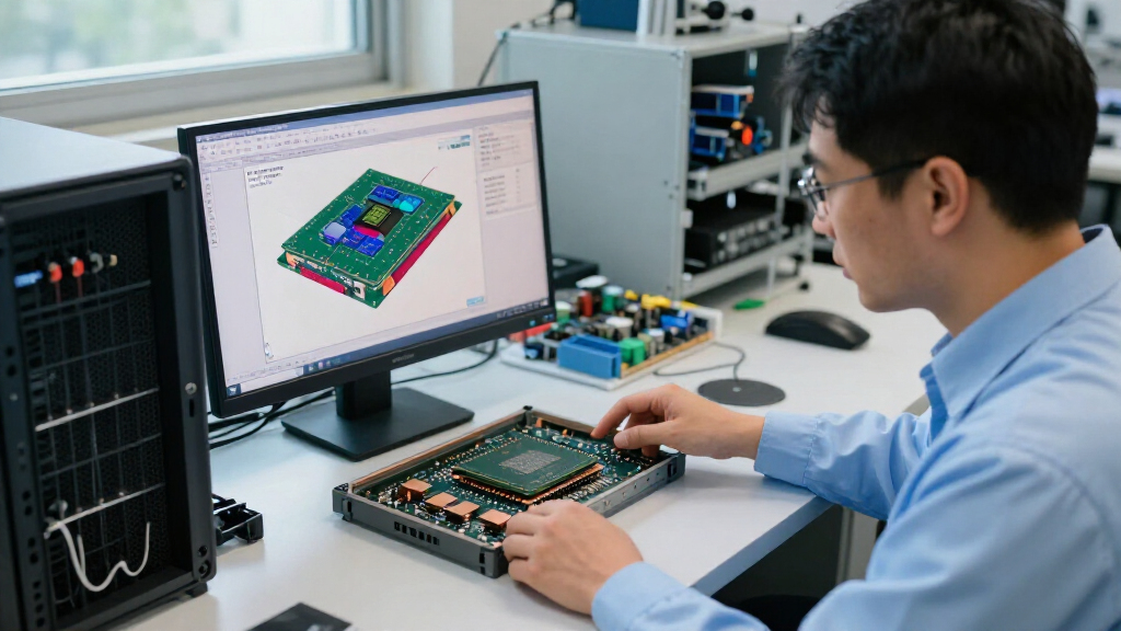
🔍 Read the full analysis: A 3D Breakdown Of The Dies And HBM Inside AI Chips on ThorstenMeyerAI.com
TL;DR
ThorstenMeyerAI.com published a 3D explainer showing how AI accelerators combine compute dies, stacked high-bandwidth memory (HBM), silicon interposers and cooling hardware. The report connects package design to rack-scale systems and argues that memory bandwidth and advanced packaging, not just compute, shape AI capacity; several dimensions in its models are schematic because manufacturers do not publish them.
ThorstenMeyerAI.com published a 3D breakdown of AI accelerator hardware on November 22, showing how compute dies, stacked high-bandwidth memory (HBM), silicon interposers and cooling fit together inside modern systems. The report’s central point is that AI performance and supply depend on more than the processor: memory bandwidth and advanced packaging also affect how quickly accelerators can be built and run.
The explainer follows an accelerator package from its base upward: a package substrate connects it to the module, while a silicon interposer provides dense wiring between compute dies and HBM stacks. HBM consists of DRAM chips stacked vertically and joined by through-silicon vias (TSVs). A cold plate sits above the package to carry liquid cooling. The report says its CAD models show the order and count of layers, but use schematic dimensions: Nvidia and AMD do not publish the millimetre measurements for these dies, packages or memory stacks.
The report contrasts designs from Nvidia and AMD. It says Nvidia’s Rubin GPU uses two reticle-limited compute dies and cites Nvidia’s product page for a memory bandwidth figure of 19.2 terabytes per second. AMD’s MI355X is described as having eight stacked accelerator complex dies, two I/O dies and eight 12-high HBM stacks. These configurations are distinct product designs, not a single common layout for all AI chips.
At rack scale, the report describes Nvidia’s GB200 and GB300 NVL72 systems as containing 72 GPUs and 36 CPUs, distributed across compute trays, alongside NVLink switch trays, management switches and power shelves. It cites Nvidia documentation for those component counts and for 120 kilowatts of cooling capacity for a GB200 NVL72 rack. These are attributed specifications; the explainer’s illustrative rack outline is based on an Open Compute Project listing.
Why Memory and Packaging Limit Capacity
The hardware layout matters because compute dies need data delivered quickly enough to use their processing capacity. HBM’s proximity and bandwidth help move data between memory and compute, while the interposer supplies the large number of connections required inside a compact package. That makes performance a system-level issue rather than a measure of processor speed alone.
Packaging can also constrain how many accelerators reach the market. The report cites TSMC’s account of its CoWoS packaging technologies and notes that making larger interposers and integrating more dies is a manufacturing challenge. It also quotes SK hynix’s expectation that HBM demand will exceed supply through 2030. That is the memory maker’s forecast, not a guarantee of future shortages or pricing. For companies planning AI infrastructure, the practical consequence is that processor availability, memory supply, packaging capacity and cooling requirements all need to be considered together.
Popular right now

Bose QuietComfort Ultra Headphones Gen 1, Lunar Blue

De'Longhi Classic Signature Espresso Machine with Adjustable Milk Frother

Breville Bambino Espresso Machine, Brushed Stainless Steel
As an affiliate, we earn on qualifying purchases.
From Silicon Interposer to Rack
The report describes the silicon interposer as the connection layer between compute and memory. TSMC says its CoWoS-S technology uses a large silicon interposer to accommodate functional dies and HBM cubes. The source says that version can support an interposer up to about 2,700 square millimetres, or 3.3 times a standard reticle area. For larger packages, CoWoS-L uses silicon bridges in a carrier layer. The article attributes production-size statements to TSMC, including a CEO’s October 15, 2026 comment that the company was in real-world production of five-times-reticle designs and working on larger sizes.
The HBM stacks are evolving too. The report cites SK hynix’s description of a 12-layer stack using thinner DRAM chips and Samsung’s statement that its 12-high HBM3E reached a seven-micrometre gap between chips. JEDEC’s HBM4 standard, published in April 2025, allows stacks of four, eight, 12 or 16 layers and up to 64 gigabytes per stack. These figures describe product claims and a published standard; they do not mean every accelerator uses the maximum stack height or capacity.
At the system level, a rack combines many packages with networking, power and liquid cooling. Nvidia’s cited GB200 NVL72 layout includes 18 compute trays, each with two Grace CPUs and four Blackwell GPUs, plus nine NVLink switch trays. The report says coolant runs through cold plates attached to CPUs and GPUs. This helps explain why the transition from a chip package to a working rack also requires substantial facility infrastructure.
What the Models Cannot Measure
The 3D models are schematic in physical size, according to the report; they are intended to show layer order and component counts, not exact dimensions. The source also combines specifications for different products and generations, so a figure for Rubin should not be read as a specification for AMD’s MI355X or for every accelerator.
Some forward-looking statements remain forecasts. SK hynix’s view of HBM supply through 2030 does not establish how shortages, prices or production will develop. The report does not quantify how much packaging capacity is available across suppliers or how much each manufacturing constraint limits shipments. It also does not provide a comparable measure of real-world AI performance across the systems discussed.
Capacity and Product Generations Ahead
The next developments to watch are the rollout of newer accelerator packages, changes in HBM stack capacity and the expansion of advanced packaging production. The source says AMD’s MI450X and MI455X use CoWoS-L and describes Nvidia’s Vera Rubin NVL72 as listed “Available Now” on Nvidia’s site. Those statements reflect the source’s account at publication; availability can vary by configuration, supplier and customer.
Further manufacturer disclosures could clarify package dimensions, production volumes and the timing of larger interposers. For buyers and infrastructure operators, the immediate questions are whether memory and packaging supply can keep pace with accelerator demand, and whether data centres can provide the power and liquid cooling required by rack-scale systems.
Key Questions
What does HBM mean in an AI accelerator?
HBM means high-bandwidth memory. It is DRAM arranged in vertical stacks and connected by through-silicon vias, allowing high-density connections to nearby compute dies.
What does the silicon interposer do?
The interposer is a dense wiring layer that connects compute dies and HBM stacks inside the package. It carries many connections that would be difficult to provide with a conventional circuit board.
Are the 3D models drawn to exact physical scale?
No. ThorstenMeyerAI.com says the models show layer order and component counts, but use schematic sizes because manufacturers do not publish the relevant dimensions in millimetres.
Why does packaging affect AI capacity?
Advanced packaging joins compute and memory into a working unit. Limits on interposers, HBM and package assembly can affect how many complete accelerators can be produced, alongside chip manufacturing and cooling capacity.
How many GPUs are in the Nvidia NVL72 rack described?
The report cites Nvidia documentation describing 72 GPUs and 36 CPUs in the GB200 and GB300 NVL72 rack configurations. The rack also includes networking, power and cooling equipment.
Source: ThorstenMeyerAI.com